Infrastructure & Security · Oct 30, 2026
Edge NPU licensor Ceva takes the same design into the data center
The next-generation NeuPro adds an "Ultra" tier aimed at AI infrastructure. Memory has become the bottleneck in LLM inference, and chip designs are emerging that put NPUs inside memory and networking chips as well
Seiichi Tanaka · Editor-in-Chief
Key points
- Ceva unveiled its next-generation NeuPro on October 28 and said it will move into AI infrastructure with NeuPro Ultra, aimed at the data center (primary source: press release)
- The same NPU architecture and software run from the edge to the data center. CEO Panush said customers can "build once and deploy across their roadmap"
- Memory and bandwidth are the bottleneck in LLM inference, so chip designs are emerging that put compute inside memory and networking chips as well. Chipmakers can license an NPU instead of building one from scratch
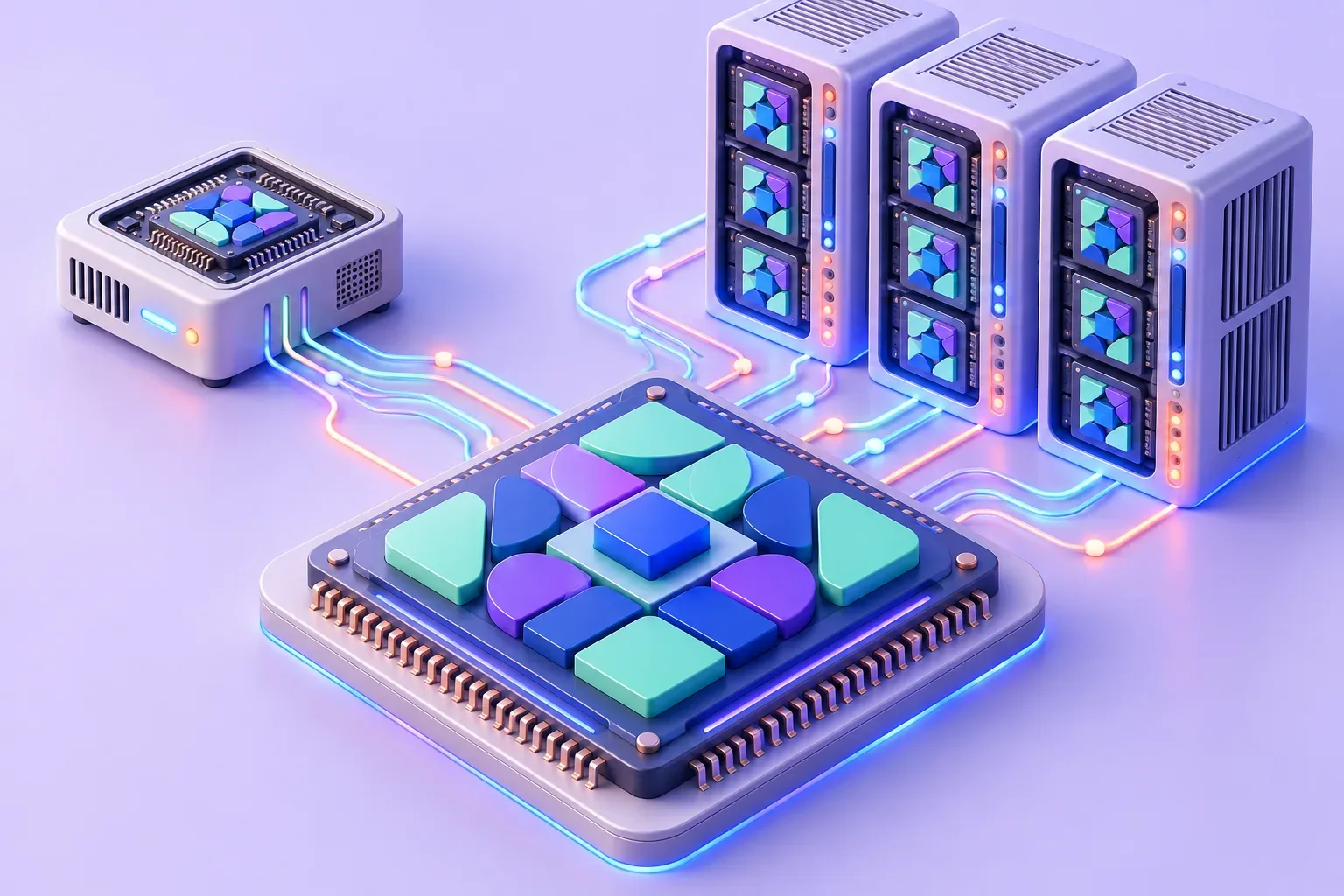
Israel's Ceva, which has made its business selling NPU (dedicated neural processing circuit) designs for smartphones and sensors, is moving into the data center. On October 28 the company unveiled its next-generation NeuPro and said it would expand into AI infrastructure with "NeuPro Ultra," aimed at data centers (press release, primary source). According to the company, everything from its small edge NPUs up to Ultra shares the same core architecture and SDK.
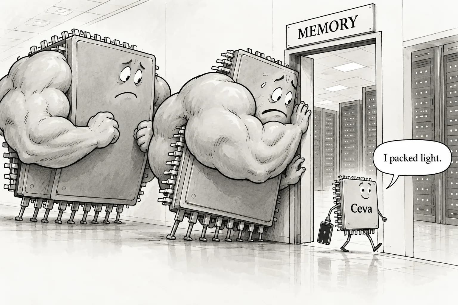
Ceva does not make and sell chips itself. It licenses circuit designs (IP) that other companies build into their own chips. So when Ceva says it is "entering the data center," that does not mean its products will sit on the same shelf as NVIDIA's GPUs. It means Ceva will pitch its NPU as a building block to companies that make data center chips.
Same design and software from the edge to the data center
The most important part of the announcement is not the new product but the fact that every product now shares the same underlying design. CEO Amir Panush said:
A common NPU architecture and software stack across every class of AI workload lets our customers build once and deploy across their roadmap. NeuPro Ultra brings that platform into AI infrastructure, an important step in Ceva's strategy to put neural processing into a broader range of semiconductor products.
The "build once" here refers to the chipmaker's software. Using an NPU requires a compiler that converts trained models for the hardware, plus a runtime, and that work is just as heavy as designing the circuit. If the same SDK covers both chips for battery-powered devices and chips that sit in data centers, customers can reuse their tools and their accumulated know-how across both product lines. Panush describes the announcement as a step in the strategy to put neural processing "into a broader range of semiconductor products."
In LLM inference, memory is the bottleneck
Why would a design built for the edge work in the data center? The answer lies in what is holding LLM inference back. As models grow and agents carry long contexts through repeated rounds of inference, the problem shifts from compute speed to how much data — weights and intermediate state — has to be moved from memory, and how fast. Adding more compute units does not cut the time spent waiting for data to arrive.
That has given rise to designs that put compute close to the data. Small NPUs are placed inside memory chips, or inside the networking chips that relay data, so that data can be processed in place before it is moved. The subtitle's reference to putting NPUs inside memory and networking chips points to this trend. These chips are not the GPU at center stage. They play supporting roles under tight power and area constraints, and they need circuits that compute efficiently within those limits. Those are the same conditions Ceva has long worked under in smartphones and sensors.
No need to build an NPU from scratch
Many companies that make memory and networking chips have little experience designing NPUs in-house. That is where Panush is pitching.
Customers building silicon for these markets can draw on Ceva's architecture, software and experience rather than developing an NPU platform from scratch.
Building not only the NPU circuit but also the software that runs it entirely in-house is a heavy lift. Licensing saves that cost and time. For Ceva, it is a way into data center chips without going head to head with GPUs.
Lessons from more than 15 first-generation customers
Ceva says more than 15 customers have licensed the first-generation NeuPro. Yaron Galitzky, executive vice president of its AI business, described what the company learned:
Working closely with the more than 15 customers who have licensed the first generation of NeuPro has shown us that successful AI products depend on the right balance of compute, memory, bandwidth, power and cost for each use case.
The idea of balancing compute, memory, bandwidth, power and cost applies just as well in the data center. In LLM inference, raising compute speed alone does nothing if memory and bandwidth cannot keep up. Ceva is using its edge experience of striking that balance for each use case as a selling point for the data center.
What to watch
Whether Ultra is actually used in data centers depends on whether companies sign licenses. Ceva did not name any data center customers in the announcement. It is also not yet clear how far designs that put compute inside memory and networking chips will spread in real products. Still, with memory becoming the bottleneck in LLM inference, what data center chips need has clearly moved closer to the low-power designs honed at the edge. Ceva's announcement is an attempt to ride that shift.
Editorial cartoon